Copyright15 way cablesCopyright

This web site was designed to be best viewed on any P.C., a SmartPhone or a Tablet.

The NE-555 Tutorials and free circuits Page Banner
Copyright © January 28th 1996 - Updated October 29th 2015   ..........    Brought to you by Unitech Electronics Pty. Ltd.

Please note, if you wish to print out this page, it will require 14 sheets of standard A4 paper ( Portrait mode ). Please, be aware of this.

To the NE-555 tutorials Page number 1            To the NE-555 tutorials Page number 2

Back to NE-555 Tutorials page 2To the Datasheets page NEXT ->

NE-555 darkness alarm    NE-555 power fail alarm    NE-555 mercury switched sample & Hold    NE-555 photo-eye-alarm    Metronome sound

practice-oscillator    NE_555_cw-prac-rcvr    NE_555_760sec-timer    NE_555_schmitt-trigger    NE_555_improved-timing

NE_555_missing-pulse    NE_555_hi-lo-siren    NE_555_tape-beeps    NE_555_decision-maker    NE_555_1Hz-oscillator

NE_555_logic-probe    NE_555_extend-timer    NE_555_HEF4017 datasheet pdf    NE_555_neon-lamp-tester    NE_555_infra-red-transmitter

NE_555_lamp flasher    NE_555_improved-oscillator    NE_555_touch-switch    NE_555_switch-debouncer    NE_555_stable-monostable

NE_555_pin-differences    NE_555_temperature-ratings    NE_555_frequency-duty-cycle-calcs    NE-xxx-data-downloads    NE_555_acknowledgements.gif

For more information about the Government's A.C.M.A. web site click on C-tick info gadget (below)

NE555 DataTo the top of this pageBack to Free Circuits

CSS 555 C Data


Safety First is our priority- Be aware of 240V mains

For guaranteed low currect consumption, the NXP (Philips) CMOS version ICM-7555 Timer IC was chosen.

ICM-7555 Datasheet pdf


Schmitt Trigger

Schmitt Trigger: Figure 9 (above)

A very simple, but highly effective circuit. In this circuit, the ICM-7555 and NE-555 "cleans up" all noise on the input signal resulting in a nice clean and "squared signal" output.

Results are immediately realised when used in radio control ( R / C ), as it will clean up noisy servo signals caused by " RF " interference induced by long servo leads. As long as R1 equals R2, the ICM-7555 or the old NE-555 will automatically be biased for any supply voltage in the 5 volt to 15 volt  
( maximum 15.5V ) range.

Please note, that there is a 180-degree phase shift. This circuit also lends itself to condition 50Hz or 60-Hz sine-wave reference signal taken from a 6.3 volt AC transformer before driving a series of binary or divide-by-N counters.

The major advantages are that unlike a typical conventional multivibrator type of squares which divides the input frequency by 2, this method simply squares the 50Hz or 60-Hz sine wave reference signal without any division what so ever.

NE555 DataTo the top of this pageBack to Free Circuits


ICM-7555 Datasheet pdf

CSS 555 C Data


Improved Timing Circuit

Improved Timing Circuit: Figure 10 (above)

Much more improved stable timing output is achieved with the addition of a single transistor and a diode to the R-C timing network. The frequency can actually be varied over a fairly wide range while maintaining a constant 50% duty-cycle. When the output Pin 3 is HIGH, the transistor is biased into saturation by R2 so that the charging current passes through the transistor and R1 to C. When the output goes LOW, the discharge transistor (pin 7) cuts off the transistor and discharges the capacitor through R1 and the diode.


NE555 Pin 7

The high & low periods are equal. The value of the capacitor (C) is 100nF (0.1uF) and the resistor " VR1 Potentiometer " is 2M2 (2.2 Meg Ohms). This is but a mere example of how to configure it , R - C values are entirely dependant on the type of application, so choose your own values (within reason). The diode can be any generic small signal diode, for example the 1N4148, or 1N914 can be ideally used however, a high conductance Germanium or Schottky type of diode will minimise the diode voltage drops in the transistor and diode. (only if that is absolutely necessary for operation).

Having said that, the transistor should have a high beta  (gain) so that the R2 1K5 can be larger and still cause the transistor to saturate. The transistor can be a BC547, BC548, BC549, 2N2222 or similar gain NPN transistors.

NE555 DataTo the top of this pageBack to Free Circuits


ICM-7555 Datasheet pdf

Missing Pulse Detection
Missing Pulse Detector (A basic simple circuit): Figure 10A (above)

This transistor can be replaced with a BC547, BC549 or 2N2222. This is a very basic example but does in fact work. Try some small experimentation with the values of R and C.

Be aware that 100 ohms is not the preferred value for R1, it was placed there for a small incoming signal from a remote control over several hundreds of meters away and the filtering required for that length of cable has deliberately been left out for simplicity's sake.

The correct value if driven from another source would be determined by the amount of current and voltage applied to almost saturate the base of Q1 BC548 thus turning it "on" so in theory, R1 (presently represented as 100 ohms could be 1K or 2K2 or higher ) it is of your own choice.

Briefly, if there is a missing "pulse" to the base input of Q1 BC548 or no signal at all, it sees it as a missing pulse inverts the signal within the NE-555 and sounds a piezo DC buzzer.

NE555 DataTo the top of this pageBack to Free Circuits

CSS 555 C Data


NE-555 Hi/Lo Siren Circuit

ICM-7555 Datasheet pdf

Hi / Lo or Hee-Haw Tones: FIGURE 11 (above)

This circuit runs two NE-555 timers together to create a "Hi / Lo" tone slightly similar to a "Hee-Haw tone. The timing is set-up by R1 (12K) and R2 (1M ohm) in conjunction with C1 (0.1uF) 100nF a polycap or ceramic. One "timer" IC-1 sets the mark-space ratio of "on / off" from its Pin 3 output, feeding to pin 7 of the second NE-555 (IC-2). The second NE-555 (IC-2) forms a very simple oscillator, you can add this great effect for your children's toys. IC-2 forms as a multivibrator, delivering a set of tones provided by the voltages present at pin 7 of IC-2 and the interaction of R4 (390K) and R5 (12K) and C2 (0.01uF or 10nF), the output limited via C3 a 15uF electrolytic capacitor. Notes: It is believed that 15uF caps used at the time when the circuit was devised, are no longer made, so it is safe to use 22uF caps.

NE555 DataTo the top of this pageBack to Free Circuits


NE-555 Tape Recording Beep

ICM-7555 Datasheet pdf

Recording Beep: FIGURE 12 (above)

As you may be aware, it is actually highly illegal in this country to record any phone conversation without the "other party's" full permission. This circuit is used to keep recording of telephone conversations within the guidelines of being legal. Once you have secured the "other party's" permission to record their conversation, then this circuit device built in a box is what you will need to have on "standby" the unit "beeps" every 10 seconds.

This will not require interfacing nor connecting to the phone lines as it is a stand-alone 9V unit which fits snugly within a plastic "Jiffy-Box" (see "Jaycar" or "Altronics") . The law requires you to provide "beeps" every 10 seconds while you are recording both parties (ie: you and the person you have called) conversations. No beeps = no recording.

The output of left IC-1 Pin 3 is fed to Pin 1 of the right side NE-555, supplying a ground pin momentarily. This drives the NE-555 to produce a higher tone while on the high side of the left NE-555's "ON" cycle. The ouput from the right side (IC-2) NE-555's pin 3 feeds a signal via C3 15uF to the 8 ohm speaker. Any 8-ohm 500mW speaker will do.

NE555 DataTo the top of this pageBack to Free Circuits

Yes / No Decision Maker

CSS 555 C Data74LS73 data sheet pdfICM-7555 Datasheet pdf

Electronic Decision Maker circuit. Figure 13 (above)

Basically it's a Yes or No decision maker, a novel use of a NE-555 for use when you can't make up your mind yourself and to have a little bit of fun with.  You could also use it as an executive decision maker. To Fire an employee or not to fire them.    The NE-555 is wired as a Astable Oscillator, driving in turn, via pin 3, the 74LS7473 a Dual J - K flip-flop.

It can also be used as a "game" heads or tails whereas, pressing the SW-2 button will result in an either heads or a tails indication, it's up to you to pick and some have fun along the way and in the process and learn about electronics. Have loads of fun at parties. invent some new fun and exciting games using this simple device. When you press Sw-2 it randomly selects the 'YES' or 'NO' LED.
The LED's flash-rate is about 2KHz (Kilo-Hertz), which is much faster than your eyes can follow, so initially it appears that both LEDs are 'ON'. '  As soon as the switch SW-2 is released, only one LED will be lit.
The decision is yours to do with as you please  .Enjoy, have fun with your electronics projects, that's what it's all about!   Electronics is supposed to be fun,  so please enjoy these very simple NE-555 circuits.

NE555 DataTo the top of this pageBack to Free Circuits
NE-555 1Kz pulse output

1Hz clock Generator

This simple oscillator example uses the a ICM-7555 or a NE-555 to output 1 Hz. The frequency for either output can be easily calculated by the following simple formula :

NE-555 1Kz calculations

Note: In reality, the output frequency will display on your CRO as 1 Hz, based on the applied maths. The circuit maths suggests that a 1K pot can be used, however some are found to be 1.013K some are 995 Ohm, so with the error in tolerance of various parts, it is possible to adjust to the oscillation frequency of 1 Hz with the 1k ohm variable resistor, experiment and see what you can observe and discover. The addition of a 100 Ohm resistor in series with VR1 could make all the difference !

NE555 DataTo the top of this pageBack to Free Circuits

CSS 555 C Data


NE-555 Logic Probe with Pulse

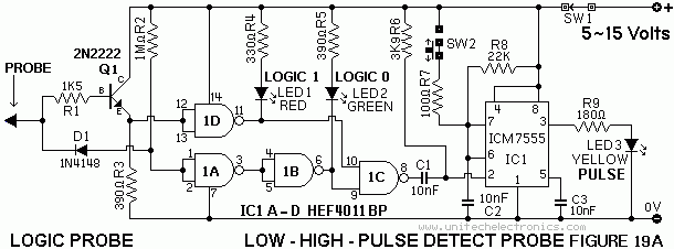
This "LOGIC PROBE" shown here as a very basic simple example of using a CMOS IC HEF 4011 and a CMOS ICM 7555 timer a CMOS version of the old NE-555 IC by NXP employing the NE-555 concept.

CD7400

Basic NE-555 based Logic Probe: Figure 19A (above)

This logic Probe provides you with three visible indicators:- "Logic 1" (+, RED LED), "Logic 0" (-, GREEN LED), and " Pulse " ( YELLOW LED ). Please note, at initial turn-on, the yellow led will "pulse" LED on/off very briefly.

In the design, the HEF4011BP was chosen as it was cheap and it had four two input NAND gates which made it ideal as there were plenty of "spare gates" to go around and, as a bonus, to employ a CMOS version of the ubiquitous NE-555 as ICL7555 to use as a "pulse indicator", a sort of "hold and display" chip. While it can be argued that the whole LOGIC PROBE could be incorporated by redesigning the circuit to eliminate the NXP ICM-7555 IC, the purpose here is to show a "NE-555" chip aka the ICM-7555 to work from 5 Volts D.C. through to 15 volts D.C.

NE555 Data

The basic circuit as it is shown above is very good for both TTL and CMOS due to voltages in excess of 15.5 Volts. Above 15.5V We may include the CMOS version at a later stage if requested. This will require a re-design of this circuit to comply with CMOS.

The yellow or 'pulse' LED comes on for approximately 190 milli Seconds to indicate a pulse without any regard to its pulse width. This feature enables one to observe a short-duration pulse that would otherwise not be seen on the logic 1 and 0 LED's. A small sub-miniature slider switch SW-2 across the R8 22K resistor with a 100 ohm R7 to limit the current to pins 6 and 7 can be used to keep this "pulse" LED feature on permanent enough after a "pulse" occurs to confirm the existence of the pulse.

In operation, for a logic ' 0 ' input signal, both the ' 0 ' LED and the pulse LED will come 'ON', but the 'pulse' LED will go off after about 190 mSec. The logic levels are detected via resistor R1 (1K), then amplified by Q1 a NPN, Silicon transistor Q1 set as a pre-amplifier and driver and selected by the 4011 IC for what they are. Diode D1 is a small signal diode to protect the HEF4011BP and the LEDs from excessive "inverse voltages" during capacitor discharge.

For a logic ' 1 ' input, only the logic ' 1 ' (red) LED will be 'ON'. With the switch SW-2 closed, the circuit will indicate whether a negative-going or positive-going pulse has occurred. If the pulse is positive-going, both the ' 0 ' and 'pulse' LED's will be on. If the pulse is negative-going, the ' 1 ' and 'pulse' LED's will be on.

NE555 DataTo the top of this pageBack to Free Circuits


NE-555 Extended Timer

Basic NE - 555 based Extended timer: Figure 23A (above)

VR1 together with R1 control the pulse rate from the ICM-7555 or NE-555, C1 10uF set the timing.  Output from Pin 3 of IC 1 NE-555 travels to the clock input of IC 2, HEF4017. Please note: On IC2, IC3 and on IC4 pin 12 is an output referred to as "carry Enable". The resultant timing is, from IC-1, 10's, from IC-2 100's and from IC-4 1000's in delays. The 4017 sequentially makes 1-of-10 outputs high while others stay in a "low" state in response to inward clock pulses. Many applications count on the 4017. The actual counting occurs when pin 13 and 15 are low logic level. Switch SW-2 is used to reset or activate and run the timers. SW-1 switches + 9 Volts power.


HEF 4017 Decade Counter/Divider

NE555 DataHEF4017 data sheet pdfBack to Free Circuits


The Basic NE-555 Circuits :

Have fun with electronics with different sounding devices, different indicating devices such as lights, LEDS, noise making devices, relays. Try different types of LDR's and..remember, if for some reason you get false triggering, connect a ceramic 0.01uF (=10nF) capacitor between pin 5 ( NE-555 ) and ground as well as 470uF electrolytic capacitor across the supply near the NE-555 chip's pin 8. In all circuit diagrams below, we used the LM-555CN timer IC from National Semiconductor. The ICM-7555 and NE-555 timer will work with any D.C. voltage between 3.5 and 15 volt. Do not exceed this as it will smoke-up !   Smoke is not a good look.   A 9-volt Alkaline battery is usually a good general choice.

NE555 DataTo the top of this pageBack to Free Circuits

CSS 555 C Data


The Basic NE-555 NEON LAMP DRIVER Circuit :

NE-555 NEON LAMP DRIVER

 A simple circuit to power a NEON lamp.   Primarily it was used to test 90 Volt neons where "The Tester's Safety" is a high requirement.
   
 Often in industry, we need to make choices as to what an employee can and cannot use in full safety in the workplace, this is one such 
 battery powered device. O.H.&.S. demands that everyone (including the Boss) is entitled to a safe non threatening workplace.     
 This is enshrined in industrial relations and in law.

 The R1 - R2 - C1 circuit determines the output oscillation frequency of the NE-555, thus producing a voltage at Pin 3,  just high enough 
 to power into the small 8 ohm transformer's primary windings, the secondary windings are 1K ohms. Thus testing any 90 Volts neon.

 This results in a ratio of about 125 times gain, however we all know based on the maths, that's not going to fly. What about the Losses ?

 The "theoretical voltage" of around 500 Volts AC passing through R3 10K dropping to around 180V AC is thus just enough to strike the gas 
 within the neon and therefore lighting it enough to detect whether the neon is a goer or just a bit of glass. It is not designed for continuous
 usage but as a "go or no-go tester", easily fitted into a small plastic box and power it by a 9 V battery and very portable. User friendly.

NE555 DataTo the top of this pageBack to Free Circuits


The Basic NE - 555 Infra-Red Transmitter Circuit and NE - 567 Receiver :

NE-555 Infra-Red Transmitter + NE-567 Infra-Red Receiver

A simple NE - 555 circuit is employed to primarily power an infra-red LED. Virtually any brand of NE-555 may be used here.

The VR1 - R1 - C1 circuit determines the ICM-7555 or NE-555 oscillator producing a square wave rise and fall voltage at Pin 3 driving the Infra - Red LED 1, being fed + Vcc via "R2" with a set value of 10 ohms. The NE-567 is a phased-locked loop chip.

NE-567 Phase-Locked LoopUA-741 Single Op-Amp

Check the data sheets for your infra-red LED as the current requirements will vary from manufacturer to manufacturer. You may need to increase the "R2" value to 22 ohms or more based on the operation current of the I.R. LED. (see PARTS 9 lines below)

This simple NE - 555 circuit runs on a single + 9 Volt DC power source, we suggest using a power supply for long term deployment. The circuit is designed for security use where an inconspicuous infra-red LED beam is needed. It is open to you for experimentation.

SETTING UP: Setting up is relatively easy, with power applied to the receiver portion, gently turn VR1 on the Transmitter board until the relay clicks ( chatters ) and operates fully and becomes as a fully latched-on mode. Be patient, this latching may take up to 2 seconds. We suggest using a small plastic "tube" perhaps with a small lens on the Photo-Transistor part to direct the incoming infra-red beam directly into the tube to achieve the best results. Line both the tubes up for best results, this task will require two persons. Please experiment with the same "tube" concept on the transmitter end as this will make the devices respond to directional infra-red input rather than a "splatter" of I.R. waves. Note: operating at lower frequencies affects latching times, making them slower. PARTS: Infra-red transistor - Wagner Electronics, Part No:IRR53C (clear lens) Infra-Red Diode - CQY-89 (remote control IR diode).

NE555 DataTo the top of this pageBack to Free Circuits

CSS 555 C Data


The Basic NE-555 Simple Flasher Circuit :

NE-555 Simple Globe Flasher

A simple and novel NE-555 dual globe flasher circuit to primarily power a relay that switches power to each globe in turn.
 
The R1 - R2 - C1 along with VR1 4K7 combo determines the NE-555  to oscillate slowly producing a voltage at Pin 3 
driving the base of Q1 2N2222 an NPN transistor, which in turn drives the relay that switches the two globes on and off. 

Diodes D2 and D3 provide the feedback logic 1 pulse to Pin 4 reset of the 555. C2/R4 forms a slight "buffering" function.

This simple NE-555 circuit runs on + 12V DC, the circuit is protected against back E.M.F. (Electro-Motive Force) or the 
collapsing coil voltage by diode 1N4004 D1 which is rated at 400 Volts at 1 amp.

The back E.M.F. from some coils measured by us has be witnessed on the C.R.O. to generate upwards and beyond a 
350 volts spike ! 

Applications: This circuit was designed for Security use or Vehicle breakdown dual lamp use where needed. Cop cars ?

NE555 DataTo the top of this pageBack to Free Circuits

The Basic NE-555 Improved Oscillator Circuit :

NE-555 Improved Oscillator Circuit

A simple (NE-555 inspired) ICM-7555 timer IC circuit with a vastly improved oscillation. So simple, why did we not use it before ? It uses only one resistor and one capacitor. For the purpose of the simplicity in display, we have "left off" the 0.01uF ceramic capacitor which we would usually connect from pin 5 to ground. It still functions acceptably.    The circuit draws very little current from the supply due to the exclusive use of the NXP (Philips) ICM-7555 timer IC, however the frequency of operation will in fact be
somewhat lower than a dual resistor circuits as describe in many other circuits on these pages.        

This lower frequency is mostly due to the fact that the voltage delivered by the output line from Pin 3
is about 1.7 Volts less than the supply rails.  The output is still capable of driving up to 200mA.        
Don't exceed this.  You may destroy your chip!  

The  R1 x C1  circuit determines the   NE-555   to oscillate, producing a voltage at  Pin 3  which also is fed back via R1 a 1K driving the NE-555 chip into almost perfect oscillation.  Observe it on a CRO.  
( Cathode Ray Oscilloscope )  or a DSO ( Digital Storage Oscilloscope ). This simple ICM-7555 circuit runs on + 5 V to + 15 V DC. Most circuits run very well at 15 V DC all day.  This circuit was designed to use for "reasonably" good square wave output formations. Hey !, nothing is perfect, you may need to add a few potentiometers just to trim things up and get a much better looking square wave, if that is what you want.      

NE555 DataTo the top of this pageBack to Free Circuits


CSS 555 C Data

NE-555 SIMPLE TOUCH SWITCH
The Basic NE-555 SIMPLE TOUCH SWITCH :


This simple application of the ICL- 7555 or the NE-555 is   "triggered"   on pin 2 via Q1 2N2222 NPN
transistor operating the ICL - 7555 or the NE-555 in Astable Mode. (see FIGURE 30A ).    

Static electricity aside (yes, someone will point out that there are no protection zener diodes on the transistor's input and rightfully so. However, it is drawn for simplicity. You may add zeners as you wish tothe touch plate to protect the base of the 2N2222 NPN transistor, thus protecting it somewhat.

The generated voltage is about 3 Volts less than the supply rail voltage due to   Pin 3   rising to approximately 1.7 Volts below the supply rail voltage, add to this the 0.6V loss through the diode. It is sensitive enough to pick up stray voltages such as static electricity and induce mains radiation picked up by our bodies.      
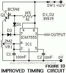
It can be "improved-on" by the addition of a second pad connected to ground which will enhance its operation.   This circuit can (  with a little experimentation  ) be connected to a metal gate or similar and be used to produce a tone using a second NE-555 circuit such as in a modified version either Fig. 1 or Fig. 2. Experiment away,   don't let your mind be "walled in" by convention and preceding circuits,   always experiment and learn. We believe Edison found 10,000 ways not to make a light bulb and one that worked. 

NE555 DataTo the top of this pageBack to Free Circuits

CSS 555 C Data

NE-555 SIMPLE SWITCH DE-BOUNCER
The Basic NE - 555 SIMPLE SWITCH DE-BOUNCER :

This mode of operation is also called MONOSTABLE MODE   The NE-555 can indeed be wired as a monostable. A monostable has one stable state and that is the OFF state.  The "unstable" state is called the "ON" or a "HIGH" LOGIC state.   When Pin 2 is triggered by an input pulse,   the monostable switches to its temporary or "ON" state. It remains in that state for a period of time determined by an   R - C   network   and returns to its stable previous "OFF" state. Put simply, the monostable circuit generates a single fixed duration pulse during each time it receives its input trigger pulse.

The monostable circuit can also be called a "ONE-SHOT" due to the single-pulse created.     This type of circuit can be used for many switching applications, activating an external device for a specific length of time.  They can also be used to generate timed delays.   Another desirable use for this type of circuit is to take the brief pulse of a   push - button   and activate a external device. We refer to this simply as a " PULSE-EXTENDER ".

Another novel use is that it can also be used to clean-up the noisy output of a push-button due to poor contacts or a high moisture area, this we refer to as SWITCH DE-BOUNCING.

The simple diagram below shows a push-button (on left) connected to a NE-555. When this push-button is pressed, you will note that a relay has been added to Pin 3 (output) the relay operates for about 5 seconds. The button must be released before the time-interval has expired otherwise the time is extended, so please note that this is a "limitation" of this simple circuit.        

NE555 DataTo the top of this pageBack to Free Circuits

NE-555 ASTABLE and MONOSTABLE MODES
The Basic NE-555 ASTABLE and MONOSTABE MODES :

FIGURE 30A and also Figure 9b ( above ) both show the ICM-7555 (NE-555) connected as an astable multivibrator. Both the trigger and threshold inputs  ( pins  2 and  6 )  to the two comparators are connected together and to the external capacitor.  The capacitor charges toward the supply voltage through the two resistors, R1 and R2. The discharge pin, ( Pin 7 ) connected to the internal transistor is connected to the junction of those two resistors.

When power is first applied to the circuit, the capacitor will be uncharged, therefore,  both the trigger and threshold inputs will be near zero volts  ( see Fig. 10 ).    The lower comparator sets the control flip-flop causing the output to switch high. That also turns off transistor T1.

That allows the capacitor to begin charging through R1 and R2.  As soon as the charge on the capacitor reaches 2/3 of the supply voltage,  the upper comparator will trigger causing the flip-flop to reset.          

That causes the output to switch low.   Transistor T1 also conducts. The effect of T1 conducting causes R2 resistor to be connected across the external capacitor. Resistor R2 is effectively connected to ground     through the internal transistor T1. The result of that is that the capacitor now begins to discharge through R2.

NE555 DataTo the top of this pageBack to Free Circuits

Table 2 - NE-555 INPUT Vs OUTPUT      DIAGRAM 2 - NE-555 INPUTs-OUTPUTS

Check the listing in Table 2. It shows some variations in the NE-555 manufacturing process primarily by two different manufacturers, National Semiconductor and Signetics Corporation.        Check Manufacturers Table 2 - click here    

Since there are many other NE-555 chip manufacturers we suggest when you build your prototype "test" circuit first of all, using one of these two well known brands and stick with that particular brand of NE-555 model if the results are great. By all means, test many others, there may be several other brands which give you comparable results on the C.R.O. 

You may wish to specify a certain brand in your own NE-555 "circuit" project and its schematics and for a very good reason, the circuit functions " better " with one brand than another.     Always test a batch of brands to see which one gives results.

Unless you "really" know what you're doing in a critical timing circuit and of course, some do and some don't, stick with one brand.

NE555 DataTo the top of this pageBack to Free Circuits

BIG NOTICE - READ NOW - TEMPERATURE RATINGS

The absolute " maximum" ratings (in free air) for NE/SA/SE types are:

+ Vcc, supply voltage: 18V Input voltage (CONT, RESET, THRES, TRIG): Vcc

Output current: 225mA (approx)

Operating free-air temp. range: NE555 :........... 0°C - 70°C
SA555 :........... -40°C - 85°C
SE555 :........... -55°C - 125°C
SE555C :......... -55°C - 125°C

Storage temperature range: -65°C - 150°C

Case temperature for 60sec. (FK package): 260°C

CSS 555 C Data

Please folks, remember that the NE-555 chip does create a certain "noise" on the Vcc supply lines, most applications can live with this undesirable characteristic.       When designing a circuit using the NE-555, observe the suuply line on a CRO.

It is however, always wise to use "filtering" capacitors, preferably a 10uF Tantalum added to this a low ESR 100uF electrolytic and as well a 0.1uF disc ceramic capacitor to assist in "cleaning up" spurious noise generated by the   NE - 555 on the supply +ve line.

Connecting an Electrolytic Capacitor the value of between 100uF and 470uF between +Vcc supply line and ground -Vdd as well as a 10uF Tantalum ( 16V~25V ) and also utilising a 0.1uF disc ceramic just to on the side of caution.

It has been observed that the introduction of a 10uH choke in the "supply in line" does not appear to improve any further after the addition of those three capacitors.       The three capacitors it would seem suffice in cleaning up the spurious previously observed "noise" on the +Vcc supply in line.      

These three caps will greatly improve the line "condition" with the NE-555 oscillating at higher frequencies,    these "noises" can be seen quite clearly on a good CRO ( Cathode Ray Oscilloscope ). The next generation of Oscilloscopes have Liquid Crystal Screens, so what do we call them ?

These will be called D.S.O.'s. Digital Storage Oscilloscopes. They will have features beyond our wildest dreams and work well in the sampling and storage area also. The question is, how affordable will they be ? Seriously, with large scale integration, liquid crystal screen prices dropping, production increasing, why so expensive ?

NE555 DataTo the top of this pageBack to Free Circuits

NE - 555 Timer - Frequency and Duty Cycle Calculator

Enter values for Resistor R1, Resistor R2, and Capacitor C1 and press the calculate button to solve for positive time interval (T1) and negative time interval (T2). For example, a 12,000 ohm (12K) resistor (R1) and 150,000 ohm (150K) (R2) and 0.22 uF capacitor will produce output time intervals of roughly 24.698 mS (millis Seconds) positive (T1) and approximately 22.869 mS negative (T2). The frequency will be approximately 20.979 Hz.

Please Note: R1 should always be greater than 1K Ohms and C1 should be greater than 0.0005 uF. Scroll up this page for basic NE-555 information ( pin-outs & many interesting NE-555 circuits devised for your interest).QU: Why do we refer to figures as "about", "approximately" and "roughly" ? ANS: On paper it all looks fine, reality is different.

The Maths of any circuit looks fine on theoretic paper, however the final results once built are not always what you desired and will need "tweaking" to get your circuit to operate exactly as you designed, largely due to component tolerances and behaviour in a circuit.

NE555 calculations

REMEMBER:   Do not run an older 1971 - 1979 NE - 555 in excess of 200KHz, it will eventually smoke-up.

Notes:   This only applies to the older NE - 555's smoking-up. The newer 1979 onwards do not have this problem.

R1 (K Ohms)
R2 (K Ohms) x 2
C (MicroFarads)
T1 (Milliseconds)
T2 (Milliseconds)
Frequency (Kilohertz)
          The Ubiquitous NE - 555 Timer Calculator ( above )
NE555 example of calculator
 Above is an example of how a 1 Hertz (clock) frequency was derived, No pun intended :-)

NE555 1 Hz Oscillator

NE555 DataTo the top of this pageBack to Free Circuits


Acknowledgement

Portions of this particular web page were extracted from our own private collection of circuit notes and our own experiments since 1976. Most are based on old circuits, however the ubiquitious NE-555 has lived on and survived obsolecence and undegone improvements to be a viable option today and.....to be re-invented as ICM-7555 by NXP (Philips) and also as a programmable CMOS version as CSS-555 made by Custom Silicon Solutions Inc. since 2009.   From such humble beginings at SIGNETICS to a plethora of options in timing, oscillation and manufacturers today.  Well done    Mr Hans. R. Camenzind !     Well done sir .

CSS 555 C Data


Layout is Copyright © 1996 Unitech Electronics Pty. Ltd. ALL RIGHTS RESERVED.

First updated: Copyright © January 28th 1996 - © 2017 onwards.

Click below to go to page 1                                                  Click below to go to page 2
To the NE-555 tutorials Page number 1            To the NE-555 tutorials Page number 2

To our other Electronics and CAD services pageTo our other Electronics and CAD services page

To the Free circuits page

sales@unitechelectronics.com

Concept-Design-Layout-Copyright-Shipping

<- Back to the main index pageBack to NE-555 Tutorials page 2To the top of this pageTo the Datasheets page NEXT ->

To the 216 HTML colors page